


Discrete 8 Bit CPU Project
Inspired by the efforts of Ben Eater and James Bates, I
decided
to build a custom 8 bit CPU from mostly discrete logic.
Introduction
While I've known how to piece together discrete logic for years (after all, I got started with computers in the mid 80's, my first computer being the 6502-based Apple II), I really enjoyed Ben Eater's video series during which he described -- in painstaking detail -- his effort to create a basic 8 bit CPU from discrete logic devices. Unfortunately, while technically an "8 bit CPU", Ben's design only supported a 4 bit address bus and a 4 bit opcode and hence could only address 16 bytes and provide for 16 instructions. Even for a "basic" CPU designed primarily to assist in the process of learning digital logic design rather than any "real world" software development, I found this far too limiting to be worth the effort to build it myself.
It wasn't long before I found another guy with a YouTube channel, James Bates, who apparently thought as I did. He wound up making several improvements to Ben's CPU including support for an 8 bit address (and hence access to 256 bytes of memory), support for the isolation of program and data memory (i.e. a harvard architecture), an 8 bit instruction encoding scheme, and the inclusion of an ALU based on the 74F382 as required to support several basic arithmetic operations. James also produced a custom assembler for the project to allow him to write programs in assembly, rather than machine code directly.
James' project was enough of a leap forward that I considered building his CPU but I ultimately decided against doing so for several reasons. First, I knew that James' CPU would take up even more space than Ben's CPU and I didn't have a tremendous amount of horizontal space in which to store the finished project. Second, a quick run through the parts lists revealed that many of the parts were expensive and the 74F382 in particular was no longer available from reputable suppliers. But perhaps the most significant reason I decided not to build the project was the need to meticulously cut, strip and fit hundreds of wires. Through the magic of editing both Ben and James significantly downplayed the investment in time required to physically build the CPU.
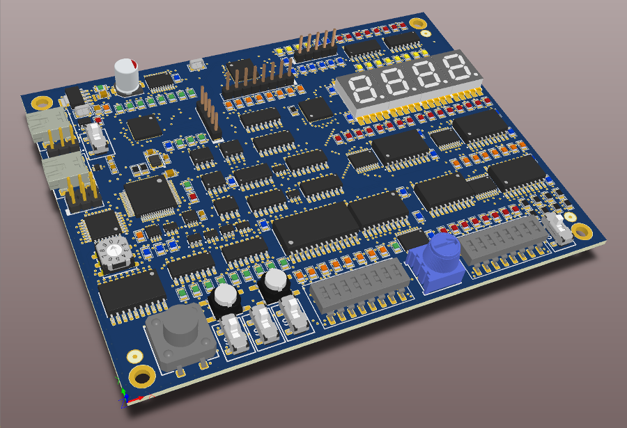
Under normal circumstances I probably would have moved on to other projects with a greater bang for the buck but I kept thinking about ways to bring the project to more people like me who have neither the time nor the patience to physically build it but have a desire to learn about basic CPU design, build toolchains, and write software (however fundamental) for it. So I came up with my version of Ben and James' CPU, based on a PCB. I have since developed a full set of schematics, and laid out the board as shown above.
SMD Vs. Through Hole
Not long into the design process it became clear that I could not cost-effectively produce a full or even semi-through-hole design, particularly one based on HUGE dual inline packages, so the first task involved ensuring I could source all components in surface mount packages. Interestingly, I found all of the HCT logic James specified available in SMD packages, but that became a moot point after I was forced to move the design to 3.3V (LVC) logic. At the end of the day I managed to incorporate only a few through-hole parts, and most of those are required only for debugging. Production will require hand soldering of a relatively few pins.
ALU Implementation
The lack of availability of the 74F382 spurred a short research effort determined to find an alternative implementation. After I figured out that discrete ALUs haven't been made in decades (or so it seems) I briefly entertained the idea of building the equivalent ALU with discrete parts. Once I realized that would be cost prohibitive I was left with the only realistic option: a small FPGA.
After reviewing the FPGA landscape I came across some full-featured and yet cost-effective Lattice parts (the MachXO2 family). While officially classified as a CPLD by some suppliers including DigiKey, they are marketed (and indeed physically constructed) as true FPGAs. Meaning, that they support the creation of sequential as well as combinational logic in an HDL (VHDL or Verilog).
I found these parts also provided several critical features I did not see in any other FPGAs:
-
internal non-volatile configuration memory (hence no need for an external flash device)
-
internal LDO required to convert 3.3V to the 1.8V required for the core (thus eliminating the need for an external LDO and supporting components required for stability)
-
internal oscillator (thus negating the need for an external crystal and high quality capacitors)
Needless to say, all of these features combine to eliminate a number of components that would easily match or exceed the cost of the FPGA itself. Lattice has got the right idea here, and other manufacturers would be well advised to follow suit. Unfortunately Xilinx and Altera (ne, Intel, or whatever they're called this week) are too busy getting drunk off the profits selling high end FPGAs to care about the little guy.
I originally expected to implement Register B (which is fixed, much as it is in James' design, as one of the two ALU operands) as discrete components. However, as layout progressed and the board got smaller I ultimately realized that the discrete devices would take up a lot of space, complicate routing, and increase cost with no practical benefit aside from nostalgia so I decided to eliminate them in favor of a few extra lines of Verilog. As a result, the ALU FPGA also contains the logic needed to implement Register B.
As James' design was based on fixed function ALUs he had to resort to a few tricks to implement all of the associated flags (carry, overflow, negative and zero). Since I was able to implement the flags as discrete signals routed to the control logic I was able to assign a full four bits of the ALU opcode to serve as function selectors. This allowed me to implement 16 functions, all of which may be redefined by the end user due to the programmable nature of the FPGA. My preliminary ALU function list follows:
| ALU Function | Selector Bits | Shorthand Name |
| Addition (A+B) | 0000 | A_PLUS_B |
| Subtraction (A-B) | 0001 | A_MINUS_B |
| Add with carry (was A*B) | 0010 | A_PLUSC_B |
| Sub with borrow (was A/B) | 0011 | A_MINUSC_B |
| Logical Shift Left (A<<B) | 0100 | A_SHFTL_B |
| Logical Shift Right (A>>B) | 0101 | A_SHFTR_B |
| Increment A (was: Rotate Left) | 0110 | INC_A |
| Decrement A (was: Rotate Right) | 0111 | DEC_A |
| Logical AND (A&B) | 1000 | A_AND_B |
| Logical OR (A|B) | 1001 | A_OR_B |
| Logical XOR (A^B) | 1010 | A_XOR_B |
| Logical NOR (~A|B) | 1011 | A_NOR_B |
| Logical NAND (~A&B) | 1100 | A_NAND_B |
| Logical XNOR (~A^B) | 1101 | A_XNOR_B |
| Greater Comparison (A>B) | 1110 | A_GRTR_B |
| Equal Comparison (A==B) | 1111 | A_EQUAL_B |
Incidentally, if you're interested in discrete ALU design, check out this article. Not surprisingly, the author also mentions Ben's work as inspiration and you will definitely see the family resemblance.
Control Logic Implementation
As I became familiar with the MachXO2 devices it became clear that they could and should also replace the EEPROMs in both the Register A / Digital Display and the control logic sections of the design. This had several positive effects:
-
Reduction of the PCB area
-
Elimination of DIP sockets required to allow the devices to be R&R'd for programming during production and subsequent experimentation
-
Reduction in labor required to separately program and insert the parts, as well as hand soldering of the sockets
The Register A implementation was straightforward and allowed me to incorporate the discrete counter and BCD to 7 segment decoder logic in a single device, which offset the somewhat higher cost of the surface mount 7 segment displays. I had a similar epiphany with respect to the discrete buffer and register as I did for Register B, and thus eliminated these components in favor of a bit of Verilog. The Register A and B changes represent the bulk of the optimization in the design.
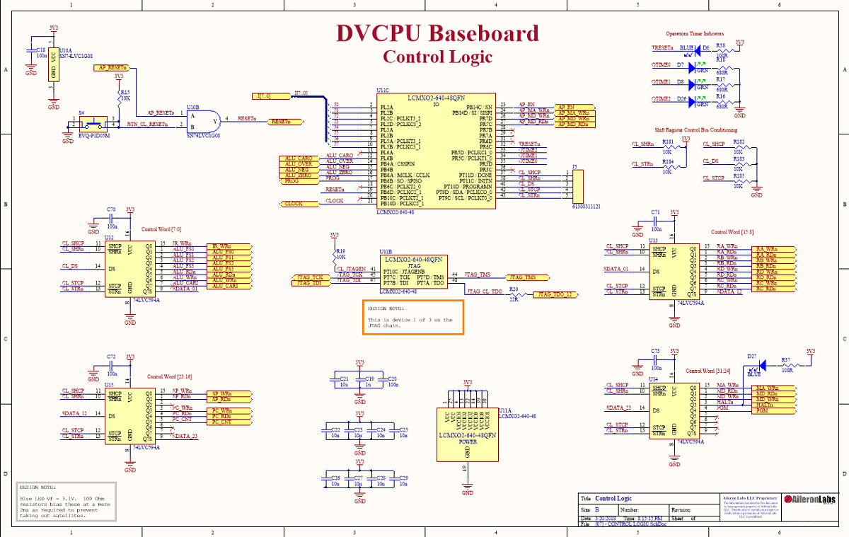
Unfortunately, while I managed to fit the ALU and Register A/Digital Display logic into the cost-effective 48 pin QFN package, the control logic wound up requiring more I/O. I could have selected the next higher pin count device, but this would have been a two edged sword -- not only did the larger part cost more per unit than the 48QFN, the resulting reduction in order quantity of the 48QFN would have driven the cost of that part up as well. So I ultimately decided to implement the control logic on the same 48QFN package and write some Verilog to drive a set of external 594A shift registers, the cost of which was mitigated by their use on the ALU / Register B LED indicators as well.
The perk of the 594A external shift registers is that they are constructed with two internal registers -- the shift register itself which accepts one bit for every "shift clock" pulse, and the storage register which uses a separate "storage clock" to latch all bits currently set in the shift register. This single latch effort updates all of the outputs simultaneously and effectively eliminates the problem James and others experienced as a result of the EEPROM outputs being undefined for a period of time following any input change. However, truth be told, James solved that problem by switching to a double-data-rate (DDR) technique that increments the instruction operation timer on the falling edge of the clock, which has the effect of driving the outputs as required well in advance of the rising edge of the clock upon which all of the other devices depend. I implemented the DDR approach as well, so in any case the CPU will be stable even at the maximum clock rate.
Manual and Automatic Programming
While the designs developed by both Ben and James relied upon DIP switches to enter the program code, it doesn't take a particularly astute observer to note that this is a tedious and error prone process. Still, some might consider manually programming the CPU a rite of passage, or even enjoyable, which explains why my design retains the DIP switches. Of course this is not to suggest DIP switches are ideal in this application or that I didn't consider alternatives.
The most obvious issue is that DIP switches are simply not designed to serve as keyboards. The average DIP switch MTBF is 1000 cycles -- meaning, each switch can, on average, be actuated a mere 1000 times before it becomes unreliable or fails entirely. I selected some high(er) quality DIP switches that are rated for 5000 cycles but this did not negate the need to implement a more reliable and less tedious method to enter program code. And so I developed one of the unique features in my design called, appropriately, "Auto Programming".
It turns out that programming the asynchronous SRAM is as simple as setting both the address and data pins of the SRAM device accordingly, asserting the write enable and then pulsing the clock. Assuming the DIP switches are disabled so they don't interfere with the process, the address signals are set via the memory address register and the data comes from the bus. So in order to program the SRAM I needed a separate device on the board to drive the control signals and the bus. Toward this end I added an Atmel (ne, Microchip) 328P, otherwise known as an Arduino, to the design. Naturally, the logic on the Arduino can read the SRAM contents as well, which means a write/read/verify operation is possible. This will allow me to write test patterns to the SRAM on power up to verify its sanity as well as zero the SRAM so any manual programming will be easier.
For a few hours I toyed with the idea of replacing the DIP switches entirely with a capacitive touch sensor IC and a specially designed portion of the PCB, but discarded that idea when I realized the cost involved and the potential impact on EMC. After all, capacitive sensor PCBs, if not implemented perfectly, can sing at frequencies that will cause a failure in FCC / EU EMC testing.
UART and JTAG Interface Programming
For production I needed a quick and easy way to load all of the firmware onto the board. This included the bootloader for the 328P, the "sketch" for the 328P, as well as the code for the FPGAs.
To facilitate programming of the 328P bootloader I implemented a standard ICSP header footprint. While the 3D view shows this header populated with 100mil male pins, ultimately the footprint will not be populated on production boards. Instead I will leverage the through holes in the board to locate the pogo pin adapter I plan to use to program the initial bootloader or subsequently update it.
To provide a means to burn sketches and otherwise interact with the 328P I needed access to its UART. The de-facto standard way to do this is via a USB to UART transceiver. I also needed to provide the equivalent of a JTAG programmer to program the flash on the FPGAs. As it turns out, several of the Lattice FPGA development boards use a 2-port FTDI 2232H in lieu of the official programmer so I figured I'd implement that device. Because this part had already been tested and deemed compliant with the Lattice tools I knew this would reduce design risk and ultimately lower cost for all users, including me, as the only thing required to connect the board to a PC for programming would be a $2 USB cable vs. a $170 Lattice programmer.
While I really can't stand FTDI as a company, the reality is their devices have good driver support on both Windows and Linux. In this case the drivers for the FT2232H will ultimately instantiate two logical ports on the PC and allow simultaneous interaction with both the 328P and the FPGAs on the JTAG chain.
Bus Design
According to the datasheets the parasitic input capacitance of the logic devices averages 4pF. Given the 17 devices on the bus this translates into 68 pF in input parasitic capacitance alone. Add in some capacitance from the roughly 12" long bus and we're looking at slightly over 90pF. This is about twice the standard value I might use as a placeholder for termination purposes, so the upside is I may not need to use the placeholder footprints I integrated with the design after all. Of course, if that capacitance combines with relatively low parasitic resistance (as I expect it to), ringing may be excessive. Only some bench testing of the prototype will reveal the need for any correction.
When it came to routing I originally expected to steer the bus from one device to the next, creating a kind of "S" shape as required to eliminate a bunch of stubs, but the physical positioning of the parts, largely governed by the grouping of the discrete registers and buffers, as well as the memory and user interface elements, prevented me from implementing that strategy. I wound up using an orthogonal routing pattern with the bus taking more of a "T" shape. This would be suicide for any high speed bus, but with a maximum speed measured in hundreds of KHz, I doubt this will be problem.
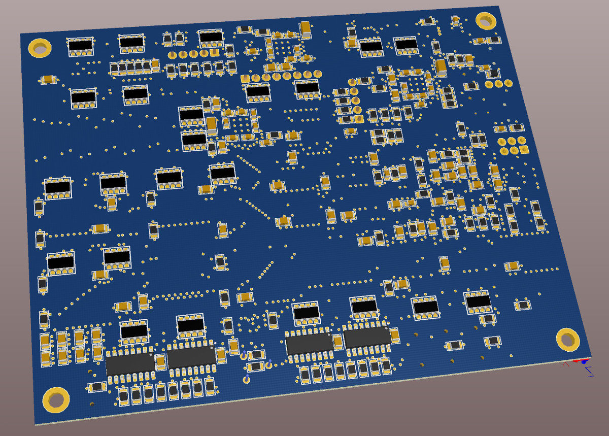
PCB and Stackup
The PCB began life as a relatively huge (5x7) board with most components on the top layer because I wanted a single sided load to make assembly of the prototypes easier. At this point there was certainly enough space between the grouped elements to permit routing on top and bottom layers, but I knew I would be better off for EMC and general routing if I used internal planes for power and ground, so I first modeled a 4 layer stackup.
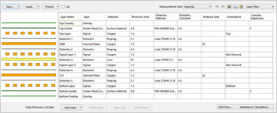
I then began a series of optimizations to reduce the overall size of the board. As expected, however, once the board was down to a decent size (ultimately 3.6" x 4.7") I realized the components, which were now nearly equally spread on the top and bottom of the board, had wrecked routing on the only two signal layers available. As a result I was forced to move to a 6 layer stackup, and even that turned out to be relatively challenging in places due to my insistence to avoid blind or buried vias. The stackup itself is custom in that I kept the signal layers at most 5 mil away from their reference planes for EMC purposes.
Speaking of EMC, I took extra measures to ensure this board would be capable of passing EMC, and in fact intend to do pre-compliance testing on it regardless of whether it goes into production, simply to verify that the techniques worked. I'll leave the details to a future update if warranted.
Project Status: ON HOLD
The PCB design is complete and awaiting prototype PCB manufacturing. However, as I have been consumed by a new job and other higher priority design work recently this project is currently on hold. Whether I continue to invest time in this project will be largely dependent upon the response from the community. If you are interested in buying a fully assembled version of this project please take a moment and let me know.