


Sunday, June 22, 2014
To CAD or not to CAD.
Last weekend I began to drill and cut the aluminum box I acquired to mount the DSPs and IsoMax units. Unfortunately, despite laying things out carefully (or so I thought), I wound up making a slight error – cutting the holes for the USB ports a bit too close to the front panel. The error only became obvious after I test fit the connectors; the solder cups of the d sub connector were too close to the body of the USB connector. Although I probably could have lived with it, I decided to take a different direction.
I had originally considered using Solidworks to model the box but figured I'd save time doing without. After all, it was just a simple box, right? Wrong. Had I modeled all the components the error would have become clear in the virtual world before I'd punched the holes in the real world. So this week I spent a bit of time modeling the box and acquiring the 3D models of the connectors I purchased so I could use them to punch holes in the 3D model of the enclosure and then send out the data to a sheet metal prototyping house for manufacturing.
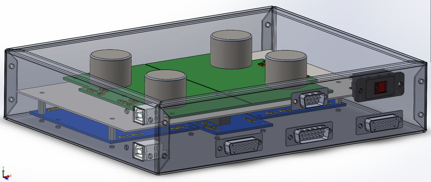
This will undoubtedly cost more than $20, but my time isn't free and you'd be surprised at how long it took me to drill, cut, and file that box to make everything fit. And still I wasn't particularly happy with the way it came out. I knew there was a reason I blew coin on Solidworks and this is it. The upside to this detour is that it will allow me to tweak the dimensions of the box to match my requirements and use steel instead of aluminum to improve shielding.
One of the reasons I gave Solidworks the nod over other less expensive tools was its ability to deal with sheet metal parts. In fact, its sheet metal facility is so intuitive that I had the box done in less than an hour – and this was my first time using it in this capacity. However, the real power of CAD is not merely in creating one's own standalone parts – it's the ability to integrate CAD models of other parts, even those produced by others, to ensure all the parts fit together properly – before they're manufactured.
To ensure the connectors would fit the enclosure properly I created what Solidworks calls an assembly, which is nothing more than a collection of individual parts. The assembly process allows “mates” to bind parts together much as if I were assembling the components in the real world. In the case of the DSP enclosure I created “coincident” mates between the front face of each connector to the rear face of the front panel and applied distance mates between the top and bottom corners of the front panel and to each of the neighboring connectors. All of the mates worked together to “lock” the connectors in place in all dimensions.
Then I edited the enclosure part and made it transparent so I could see the connectors through the face of the panel. This, in turn, allowed me to select the appropriate contours on each connector that I wanted to use as a basis for a sketch on the face of the panel that would ultimately be used to “cut” holes in the panel. There's no dimensioning necessary as the dimensions are driven by the 3D model of the connector. This guarantees that the cutouts will be the precise dimensions of the associated connectors (or slightly larger with an offset of, say 1 mm to make the fit a bit loose). And because the act of basing the cutouts on the connectors in an assembly creates implied relationships between the parts I can move the connectors on the panel later to tweak the design as necessary and the locations of the cutouts on the panel will automatically update to reflect that change. The same idea applies to changes to the dimensions of the box – everything updates automatically. Parametric modeling rocks!
Once I have the CAD model of the enclosure complete I'll send out a few RFQs to have it manufactured.
EMI Research
 Research on the topic of EMI revealed a few interesting
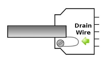
things. Looking at the MiniDSPs it's obvious that each channel has three connections
associated with it – the two differential signals (+/-) and the drain
wire or shield (s). What might not be obvious to someone new to the study of
EMI is the undesirable consequence of routing the shield wires from the harness
through the panel connectors and then to the corresponding pads on the PCB.
That is actually a very bad idea because it would defeat the purpose of the
shielded enclosure. Any noise induced on the shields and hence the drain wires
would be carried into the enclosure where they would dutifully radiate and
impact the very circuits the enclosure is designed to protect. For this reason
I knew the drain wires would need to be cut short and bonded to the case in
some way, but I didn't know initially whether it would be acceptable to keep
them as short as possible and tie them to a stud inside the enclosure in close
proximity to the connectors. This also turns out to be a bad idea.
Research on the topic of EMI revealed a few interesting
things. Looking at the MiniDSPs it's obvious that each channel has three connections
associated with it – the two differential signals (+/-) and the drain
wire or shield (s). What might not be obvious to someone new to the study of
EMI is the undesirable consequence of routing the shield wires from the harness
through the panel connectors and then to the corresponding pads on the PCB.
That is actually a very bad idea because it would defeat the purpose of the
shielded enclosure. Any noise induced on the shields and hence the drain wires
would be carried into the enclosure where they would dutifully radiate and
impact the very circuits the enclosure is designed to protect. For this reason
I knew the drain wires would need to be cut short and bonded to the case in
some way, but I didn't know initially whether it would be acceptable to keep
them as short as possible and tie them to a stud inside the enclosure in close
proximity to the connectors. This also turns out to be a bad idea.
There are two basic domains in the study of EMI: emissions and immunity. The goal of any EMI study is to minimize any emissions the product may generate and make the product immune to the emissions of other products. Since what I'm building is not a commercial product and won't be going for FCC certification I'm more concerned about immunity than emissions, but I read a paper that clarified the fact that a drain wire connected to the shield of a long cable combined with some capacitance and inductance inherent to the cable and chassis makes for a fine antenna. The article codified that the drain wire must be terminated inside the d sub backshell – on the outside of the enclosure. This practice naturally requires expensive metal backshells but I had purchased those already because I wanted to help shield the signal wires as they were untwisted inside the backshells to enter the solder cups. Unfortunately, the backshells aren't really designed to serve as a bonding point for the drain wires, however, so I'll have to come up with something custom.
If you've ever peaked inside of a piece of electronics gear you may have noticed that the cables that run between the panel connectors and PCBs are twisted. As I've known for some time that turns out to be one of the most effective ways to improve EMI immunity, and the higher the twist rate (twists per unit of length) the better. I found it particularly interesting that the shielded twisted pair cable I'm using really doesn't have a lot of twist as manufactured. That may be a simple reflection of the fact that the cables are bundled with a 100% foil shield, but with the shield removed inside the enclosure you can be sure I'll be twisting the wires to the extent possible.