


E36 BMW OBC Project
Inspired by the OpenOBC Project I've decided to fund an R&D
project to replace the main logic board in the 18 button OBC
provided as an option on E36 BMW automobiles built from
1992-1998.
The DVOBC project picks up where the OpenOBC project left off, and aims to provide a replacement for the main logic board in the factory 18 button OBC of E36 BMWs (1992-1999).
Project Goals
-
Provide functionality equivalent to the factory 18 button OBC logic board.
-
Create a modular architecture that allows the design to be flexible and expandable over time to support everything from diagnostics to data acquisition.
Product Variants
-
A fully assembled logic board option to satisfy a niche market need for this board to replace the factory 18 button OBC logic board.
Availablility: This product variant will be produced if the economic climate in the US improves and a sufficient number of pre-orders occur.
-
A turn-key product that will utilize the same logic board as in the first variant, mated to a daughtercard unique to this variant that will host a sunlight readable, high resolution color TFT display with capacitive touchscreen interface, all housed in a custom case that will replace the factory OBC in its entirety.
Availability: This product variant is not currently slated for production but may be approved at a later date based on a variety of factors, including the success of the assembled logic board variant.
Hardware Features
-
The processing core of the unit will consist of a high performance microcontroller incorporating 2MB of flash and 512K of SRAM. In addition, 1MB of external SRAM will be provided that can be used for either program memory or as a LCD frame buffer when deployed in conjunction with the turn-key product variant.
-
The board receives power from the vehicle harness and then passes that through an AEC compliant power supply fault detection and protection circuit which prevents under and over voltage, negative voltage and over-current conditions. All faults other than over-current are automatically reset. Over-current faults will be latched and require the unit be power-cycled. The over-current limit is set well below the harness branch circuit fuse rating so a current fault on the unit will not blow the vehicle's fuse.
-
The board will integrate three expansion module (EM) slots. One of the slots will be dedicated to a board that provides required K bus functionality. The other two slots will permit the installation of a variety of boards with varying functionality.
-
The X1070 and X1071 harness connections will leverage new connectors so the original connectors from the factory OBC board will not be required. A small modification will be made to one of the connectors to fit the keying of the harness connectors as the original connector is not available for sale in the aftermarket. Installation of the logic board option will only require desoldering of the OE keypad and display ribbon cables. Connections to the vehicle harness will be plug-and-play.
Developer Information
The hardware design will remain proprietary, however specifications and documentation will be provided to registered developers as required to facilitate software development.
Access to a software load supporting the assembled logic board product variant will be provided via an open source model, but support for this software will be limited to registered developers.
More information about the developer program will be released when appropriate.
FAQ:
-
Will your project provide backward compatibility with the OpenOBC project board? In other words, if I have already wired up stuff to the OpenOBC, will I be able to simply swap the OpenOBC board with your board?
Simple answer: No. My design is completely different. However, I see my project not only meeting the original design goal of the OpenOBC project, which was to replace the functionality of the factory OBC logic board, but also providing additional functionality through the expansion module interfaces, so it's likely that whatever functionality you are utilizing could be provided via an expansion module.
-
Why did you not simply take the OpenOBC gerbers and produce PCBs from that existing design?
Several components were no longer available, and replacements were not pin-compatible, hence the PCB footprints had to change. That dictated a re-spin of the PCB.
-
Why did you not simply copy the basic design of the OpenOBC and generate a new board with new footprints for the obsoleted components?
First, my technical analysis of the OpenOBC project revealed several deviations from what I consider acceptable design practices so my design aims to correct these deviations. Second, I needed to improve the modularity and functionality of the board to expand the target market for the design as required to improve my return on investment, not only in terms of monetary value but the technology I develop for this board that I can leverage in future designs, thus reducing development costs on those projects. Finally, I did not want to imply any compatibility with or support for the OpenOBC boards that may be in the field.
-
Do you plan to sell bare PCBs that can be assembled by the end user?
No, primarily because the complexity of the design and the space constraints dictated by the dimensions of the original factory OBC logic board have required the use of some package types that are challenging to reliably assemble. This option would also necessitate revealing the bill of materials and put my IP at risk.
-
Why are you producing the LCD option?
While market research has clearly indicated a demand for the assembled logic board variant, I believe the market for a turn-key solution is far larger and so the overall success of the product is more dependent on that option. As a result, I expect to develop a prototype that demonstrates the basic functionality of both variants before the logic board option is manufactured to ensure the same logic board can be used for both variants.
-
How can I buy or reserve one?
At the moment the project is in the prototype stage and I am not accepting orders or pre-orders.
Project Status: ON HOLD
May 23, 2023
I've had a surprising number of people inquire as to the status of this project over the last year. As I have stated on the bimmerforums thread I had to put this project on hold in 2020 as Covid gripped the world. What I did not realize at that time was how long and how severely electronics supply chains would be affected by the pandemic. As of today, the supply chains are recovering but are still in disarray by historical standards. Many parts are simply not available, and those that are available have either exceedingly long lead times (often in excess of a year) or are available at very high cost, to the point that it is not practical for me to engage in the engineering required of this project.
Complicating all of my electronics work is a recently announced change to the ARM IP licensing model proposed to become effective on January 1, 2024. Should this licensing model be implemented as presently designed, I will not be able to purchase any ARM-based devices after that date. This presents a significant risk to any design work involving ARM-based devices, including the STM32 microcontroller I originally planned to use in this project.
Presently the ARM company charges silicon device manufacturers like ST or NXP an IP license fee that is typically a percentage of the cost of the CPU or microcontroller I can buy from a distributor such as Digikey. Driven by greed to increase profit in preparation for an IPO, they now seek to license their IP directly to OEMs (like me) and then charge the OEM a license fee that is a percentage of their finished goods price. As the ARM based CPU or microcontroller is only a small part of the finished product and I do not believe ARM is entitled to surveil my business records nor levy a tax on anything other than the part containing the ARM IP, I will never agree to sign any license agreement with ARM under the proposed terms.
Like many in the industry, I am currently scrambling to research alternatives to ARM technology. One proposed solution involves a RISC-V soft-core based CPU and other IP cores to support interfaces such as SPI, USB, and the like, all deployed on a FPGA. This will allow me to build a FPGA-based compute module that could be adapted to multiple products but the reality is this is easier said than done. ARM is entrenched in the embedded hardware space and RISC-V solutions, while making considerable progress recently, are in their infancy. Any final solution is likely to be a year or more away as the industry comes to grips with ARM's greed and ramps up research and development on alternatives to their technology.
Unfortunately, this means the status of the DVOBC project is unlikely to change in the near future but any and all updates will be published here.
August 8, 2020
Since my last report I have managed to make a single physical change to the design -- a reduction in the overall size of the expansion module debug board (EMDebug). Since cost of a PCB is directly related to board area, cutting this board's overall dimensions will reduce its cost significantly.
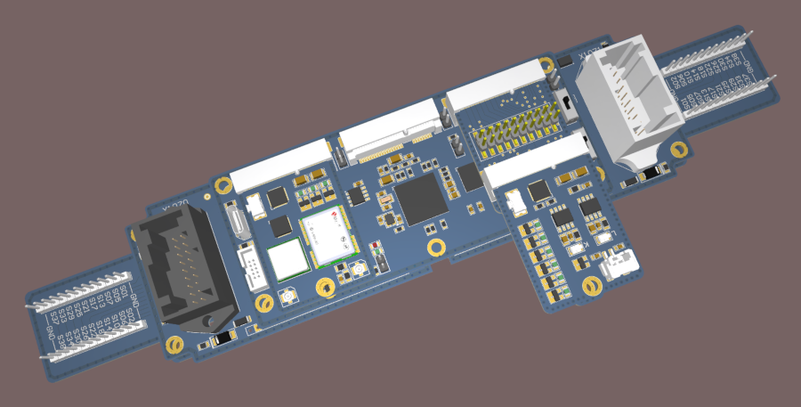
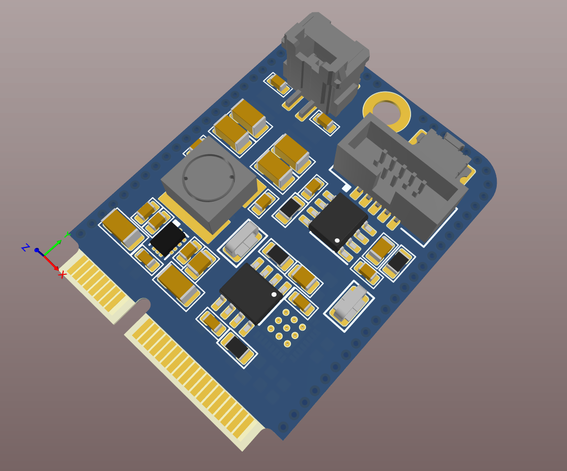
As I develop a design I select a part and then create a schematic symbol for it. If the part survives the design reviews along the way and is ultimately selected for the circuit I then create a footprint for the part including a 3D model so I can push it to the PCB design. I then conduct a preliminary layout of these parts to ensure they'll fit in the space available. If that is not the case I replace the affected parts with new ones and repeat the process. This is a bulk of the work that has been accomplished until now and has produced the 3D model you see at the top of the page.
Of course, some parts don't make it through the design reviews or BOM optimization process which attempts to reduce the overall number of parts in the design as required to reduce manufacturing and assembly costs. This leaves spare schematic symbols and/or footprints in the libraries, which I must remove to eliminate clutter so I can more efficiently check the remaining symbols and footprints for correctness.
During the last few weeks I managed to archive all of the unused symbols and footprints and am now ready to begin a review of the remaining symbols and footprints before I proceed to routing.
Project Status Change
When I started this project I committed to do one thing -- produce a prototype that was worthy of production so it might eventually be manufactured in volume -- volume, in this case, being a relative term. I knew going in the market for this project was small and I was most certainly not going to get rich building it. Not long into the project it became clear I would have to invest far more time than I would ever recover in any potential production run, but I justified continuation of the work as a passion project and because I knew a lot of the design work would be utilized on future projects.
A couple weeks ago I dodged a very large bullet in my work as a pilot that I currently depend upon for a sizable fraction of my income. Thousands of pilots like me have not been (or will soon not be) so lucky. The crack of the sonic boom I heard as that bullet whizzed by me sent a very clear message -- the economic conditions in the industry, and indeed the entire world, have changed significantly in the last six months. Worse, it appears that certain forces in this country are determined to destroy the economy for political purposes and so the V-shaped recovery I had hoped would materialize is unlikely to occur and any recovery to 2019 prosperity is likely years away.
As a result I have been forced to accelerate development of other products with a higher revenue potential. This, in turn, has forced me to change this project's status to ON HOLD to reflect the limited progress and infrequent updates that will result. This does not mean that the project is canceled. Work on it will continue as time and inspiration allows, but I clearly will not be able to commit to any timeline for completion. Any future updates or changes to the project's status will be documented here.
July 19, 2020
Over the last few weeks I've managed to do the following:
-
The baseboard outline has been modified to provide necessary reliefs at each corner to accommodate the rear cover of the factory OBC case. These changes moved the mounting holes at the four corners inward slightly, and since these are used by the recently created IO debug board I updated the outline of that board too.
-
The JTAG connector and mux used to switch between the connector and the main JTAG bus has been removed from the GWAB and DA boards. These features were intended as a failsafe so I could program these devices even if the chain on the baseboard were broken in some way but I was forced to remove these items because I simply ran out of room to place other needed components. The upside is that this has reduced BOM cost and complexity. The downside is that if the JTAG chain on the MCU board does not work as expected I'll have to develop a separate test jig to allow programming of these boards independently of the MCU board or re-spin the MCU board.
-
Status LEDs have been added to both the GWAB and DA boards. For example, on the GWAB board the pulse output of the GPS will drive an LED to serve mostly as a heartbeat and confirmation that the GPS is locked. On the DA board five separate LEDs will indicate a variety of states including those associated with the K bus and CAN bus transceivers. The parts I added are common to the BOM of several boards and can be removed in production if warranted to reduce cost but as this product is mostly intended for development at this point I think they'll come in handy.
-
While working with the GWAB and DA boards I realized that any attempt to add debug headers to these boards would fail due to a lack of space so I created an expansion module debug board (EMDebug) that will serve as a carrier for a module under test. Like the IODebug board the EMDebug board is expected to provide access to all signals so it is compatible with all modules.
-
While attempting to translate mounting holes between the coordinate systems of multiple boards it quickly became apparent that I'd need some documentation I traditionally create for manufacturing at the end of the project but I didn't have a lot of time or patience to create it at this moment. Altium's relatively new Draftsman tool looked like a quick out and sure enough I used it produce the needed documentation in a fraction of the time it would have taken doing it the old-school way, which traditionally involved drawing on various layers and publishing via gerbers. Draftsman isn't as polished as the equivalent process in Solidworks, but it is a huge leap forward for Altium. This is one less tedious process I have to deal with when I push designs out to manufacturing.
Over the coming weeks I'll planning to continue optimization of the design and wrap up the schematics review as required to begin routing.
June 11, 2020
While reviewing the bimmerforums thread on the OpenOBC project I saw a picture emblematic of early hardware design and debugging -- there were flying wires everywhere attached to a breadboard. While I have created my share of test circuits on the bench to validate much of what was designed on the OpenOBC, I was determined to make my design debuggable without being unwieldy.
Toward this end I created an IO Debug board, the purpose of which is to provide test access to the signals on the MCU-Baseboard interface as required for software debugging on the bench and in the vehicle. These signals are level shifted to 3.3V and protected against surges from the vehicle harness and are thus suitable for connection to test equipment including logic analyzers. The IO debug board has been designed so that it will securely attach to either side of the baseboard. To access both sets of signals simultaneously two copies of the board will be necessary.
One downside to test jigs is that they often cause what I call the "Schrödinger's debug" problem, an homage to the famous quantum physics thought experiment. Merely observing the signals changes what is observed. When connected to the baseboard the IO Debug board adds large stubs to all signals. On a high speed design this would be verboten because it would affect the functionality of the design, but when we're talking about baud rates instead of gigabits per second, the effects are less noticeable. The upside to my design is that the debug board retains good EMC qualities and of course reduces the mess of flying wires and the associated impacts on the design that would otherwise be required to gain access to these signals.
I have plans to build a riser assembly for the X1070 and X1071 connectors so I can connect the vehicle harness or an equivalent bench test signal to the product as required to validate the IO protection circutry. I am also planning to simplify the JTAG chain on the expansion modules, create a USB OTG expansion module and finally, design the touchscreen LCD module.
June 1, 2020
One of the downsides to reverse engineering a product is that it is easy to become myopic with respect to design improvements. Much of the design work on this project has been the result of stepping back and looking at it with a more objective eye. In the early days of my design effort the foray into expansion slots was one such example. More recently, I've developed I/O interface protection to ensure the design is resilient in a challenging electrical environment.
About a month ago, as I found myself wrapping up and doing more cleanup than new design work I realized that the design would benefit significantly from further modularization. The result is in the form of a micrcontroller daughtercard (MCUD) that mates with the baseboard. The MCUD is now host to the "brains" of the product, including the MCU and its supporting components, JTAG debug chain, USB debug interfaces and expansion slots. The baseboard remains host to the "dumb" portion of the design, including the IO protection circuitry, power supplies, high resolution ADC, and factory OBC keypad and LCD display interfaces.
This change has produced several positive impacts:
-
The overall design risk has been reduced in that I can manufacture, assemble and test the baseboard separately from the MCUD. Furthermore, I can replace the MCUD with a "dumb" breakout board that allows me to validate the IO protection circuitry without putting the expensive MCU at risk, or forcing me to partially assemble the board, as would have been the case with the original monolithic design.
-
Due to a simple lack of board area the IO protection components were previously crammed onto the baseboard in ways I knew might cause signal integrity issues but the additional room has allowed me to fan the components out in the way I originally envisioned.
-
The cost of PCBs is rooted in both size and layer count. The baseboard layer count has been reduced from 8 to 6, which will reduce its manufacturing cost. The MCUD is currently designed as a 6 layer board, but even if it ultimately requires 8 layers to successfully route it this will still be cheaper than the original design because the board is smaller than the baseboard.
-
Fewer components on each board will make them easier to hand assemble on the bench during prototyping and cheaper to assemble on automated systems in production due to fewer reels on the pick and place machine and reduced setup time for those parts.
-
The additional area available on the baseboard has permitted the reintroduction of the 5V power supply. 5V will once again be provided to the expansion slots, and this will simplify expansion module design, as well as allow me to provide an expansion card with USB OTG and limited power for USB devices such as flash drives. In a related note I am considering restoring the supercapacitor-based backup power supply as well, but I have not made a decision about that yet.
This work set me back about a month but I think the end result is worth it.
April 23, 2020
One man's stay-at-home order is another man's gold mine of time free from distractions. Over the past month I completed design and preliminary placement of two expansion modules -- what I'm calling the Data Acquisition (DA) board and the GPS/Wifi/Accelerometer/Bluetooth (GWAB) board, made a variety of significant changes to the baseboard design to accommodate these modules and resolved a major sticking point with respect to the support of analog sensor interfaces.
Each board presented its own design challenges. First, I had originally expected to sell a separate expansion board to support CAN bus but recent comments on the bimmerforums OBC thread regarding the reliability of the K-bus transceivers convinced me to put them back on an expansion module. I couldn't justify a module with only a couple K-bus transceivers on it so I decided to combine them with a couple CAN bus interfaces. Of course, once I pushed all the components to the PCB design space it became painfully obvious the board was too small to accept the components required by two CAN bus interfaces so I was forced to eliminate one of the interfaces. Considering that CAN bus is capable of supporting 50+ devices on a single network I figured this would not be a serious limitation. Doing this also freed two additional GPIOs on the microcontroller.
Normally, CAN bus requires a form of termination at both ends of the bus. This is because CAN bus leverages driver transistors configured as open-drain (or open-collector) and the termination resistors pull down the bus to a recessive state once the drivers de-assert. Devices placed between the two endpoints do not require and must not enable any termination. The problem is that because I am not designing the network I cannot know ahead of time whether the OBC will be at the end of the bus or in the middle of it, and hence whether termination should be enabled or disabled. For this reason I have implemented selective termination to be controlled via software. Termination will be disabled by default as that is the least-intrusive option should the OBC be connected to an existing (and, by necessity, properly terminated) network.
For those wondering whether I intend to provide access to an analog interface or access to ADCs in support of sensors, the answer is no, simply because of the inherent complexities in designing and protecting analog interfaces. To do this properly, all elements of the sensor output, length and type of the cable to the sensor, and other details must be known ahead of time, and this is simply not possible or practical in this application. Fortunately the market is host to many sensors that natively support CAN bus and those can be added to an existing CAN bus network easily and effectively without any additional wiring. To support sensors that only provide analog outputs the market offers many existing CAN bus conversion devices that perform the analog to digital conversion. And for those sensors that cannot be accommodated by such conversion devices, a custom external conversion device can be created and tested independently of the OBC.
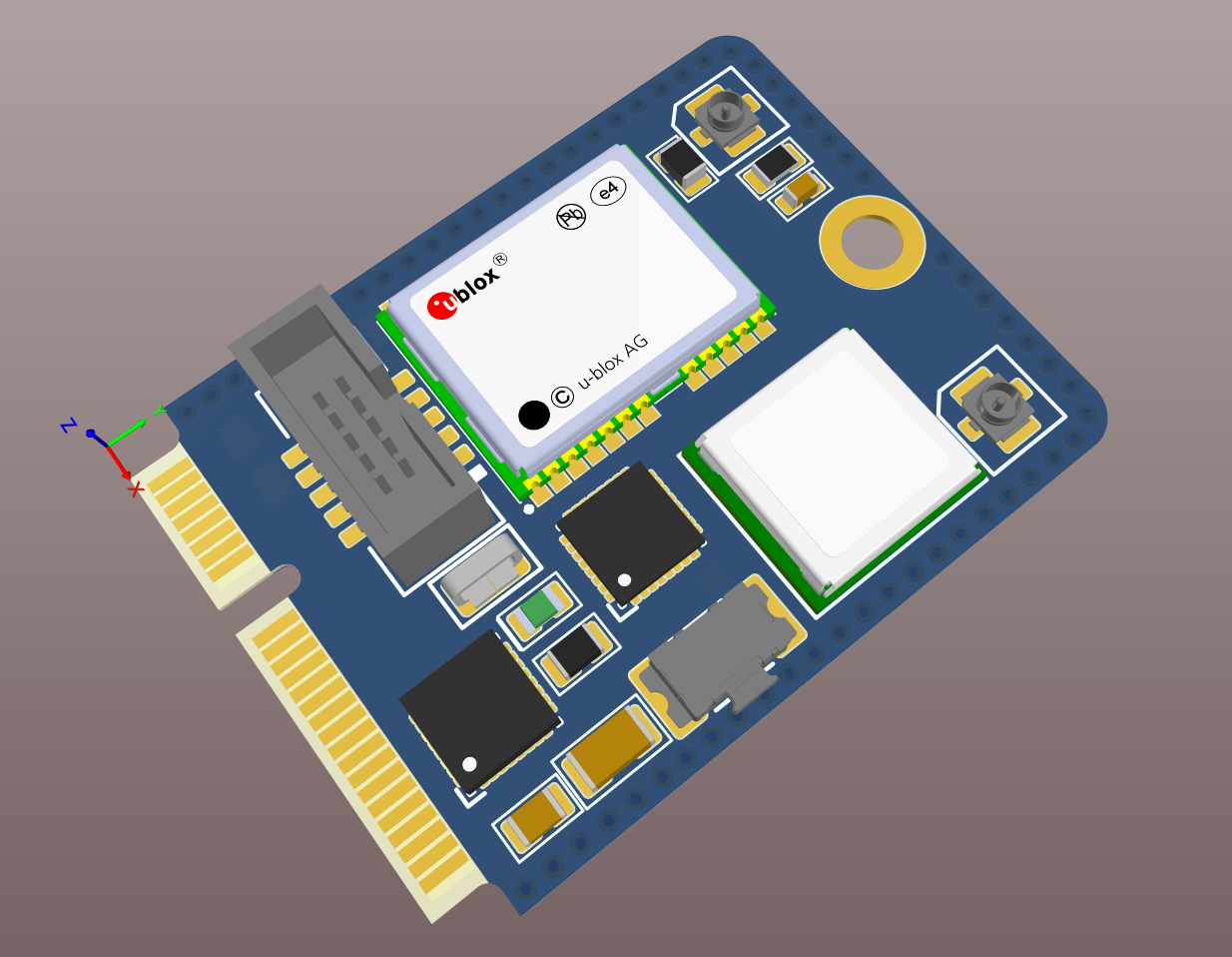
While integrating the GPS module with the GWAB board I realized that while the GPS could be configured to write its configuration to non-volatile memory and thus the GPS did not technically require a backup power supply, further research revealed that software must initiate the process; it does not happen automatically. While it is technically possible to save the configuration during initialization, this would not save the ephemeris data which is naturally acquired during normal operation, which ultimately means this data would be lost during a power disruption. Following the event the GPS would start up "cold" and take extra time to lock. As a result I decided to implement a small backup power supply that serves only the GPS.
The perk of the GPS module design is that it completely disconnects the backup power source when the module is powered via the primary bus, and since the OBC will be powered continuously (though in a low power "sleep" mode when the vehicle ignition is off) the life of the backup power supply will be limited only by its self-discharge characteristics. Incidentally, the particular GPS module I selected is automotive rated and supports SBAS differential corrections (in the US via the WAAS geostationary transponders developed for the aviation industry to allow high accuracy approaches). This combined with a preamplified antenna mounted outside the OBC case should provide outstanding position accuracy and a 10 Hz update rate.
The MachXO2 FPGA I first implemented as a reset controller on the baseboard has found a home on each expansion module in the form of glue logic. These units will manage enable and reset lines for various components on the board and multiplex interrupt signals to minimize the need for multiple interrupt lines in the baseboard-module interface. I'm planning to use the FPGA's integrated I2C slave interface (which does not require consumption of programmable logic resources) as the primary means of communications. Speed is not really a factor here (the GPS module, for example, updates its position merely ten times a second) so I2C should get the job done. A high speed UART with hardware flow control enabled will be used to communicate with the Bluetooth module, however, as this interface will be used to transfer considerable amounts of data at high speed.
One perk that resulted from the use of I2C on the Data Acquisition module is that the SPI interface for that particular slot was unused so I decided to relocate it to drive the factory OBC display. While it is is possible to bit-bang that interface much as the OpenOBC did, it's always more practical and consistent to drive it with purpose-built hardware, as that will offload this processing to hardware and thus reduce CPU utilization. The irony of this change has not escaped me. With the elimination of one of the "standard" interfaces and the addition of the K and L lines on the associated expansion module slot I have in effect created a custom interface that can serve no other board and hence recreated the supplemental module concept. Such is the nature of design.
March 26, 2020
The last few weeks have seen significant progress on the project to the point that the baseboard placement is largely complete. Of course I reached a similar milestone some time ago and wound up ripping up significant portions of the schematics, but unless the requirements change significantly I expect this to closely resemble the final product -- to the point that I updated the picture at the top of the article.
Some of the significant changes:
-
As you can see from the picture the SM slot is gone yet the board maintains three expansion slots. The location of these slots now conveniently aligns with a relief built into the factory OBC case rear cover so expansion cards should have considerable flexibility with respect to component height. You may also note that all jacks, the boot mode and power switches, and status LEDs are now usable / visible with all expansion modules populated. The MicroSD card slot has been moved from the SM to the baseboard and placed in the only available location on the top of the board that provides access to the side of the slot and thus the ability to swap cards without pulling the baseboard from the factory enclosure. These changes should make development on the board a lot easier.
-
The original plan to migrate the supercapacitor-based backup power supply from the SM to the baseboard had to be scrapped due to a lack of space for a supercap of sufficient size. I tried to integrate smaller caps to save the earlier design choice but I quickly concluded the lower runtime would not justify the cost and complexity of the feature. This means the system will not have any backup power in the event the 12V input from the harness is disconnected but recall that the board will obtain its power from the HOT bus (which is on continuously, even when the vehicle is parked and the ignition is off) so this is less of a concern. The loss of the backup power supply was further mitigated by my discovery of a GPS module that stores ephemeris data in local nonvolatile memory automatically. In short, the design no longer requires a backup power supply, but that won't stop individual modules from incorporating their own smaller supplies if desired.
-
In order to implement the turn-key product variant I originally planned to attach a LCD daughtercard to the baseboard with a common board-to-board connector over which I was free to define the interface. Although I knew the STM32F4 microcontroller supported a relatively new high speed LVDS-based serial display standard called DSI, I decided to use a common RGB parallel interface due to familiarity. Due to a recent need to leverage additional peripherals in the device and IO conflicts with the exceptional number of IOs required to support RGB I have decided to switch the interface to DSI. This limits the number of off-the-shelf displays I can use but there are several upsides. First, the connector size is significantly smaller and less expensive. Second, this frees a lot of GPIO I can use to eliminate the need for IO expanders, which while simple in concept do require more software development to leverage. Third, DSI can be turned back into RGB on the daughtercard using either off-the-shelf ICs or an FPGA and some freely available IP so this in no way boxes me into a corner should I ultimately decide to produce the turn-key variant.
-
I integrated a small FPGA, the Lattice MachXO2, as required to implement a programmable reset controller. This device will take input from either the MCU or a physical button and reset all devices in a deterministic order and timeframe. This will minimize surge currents during reset operations which can cause glitches when devices drop below their undervoltage protection thresholds and produce noise detectable during EMC testing. This device may also serve an important role in controlling the boot mode pins and reset of the MCU during an OTA firmware update but research on the subject is not yet complete.
- The SRAM package has been replaced with a much smaller BGA package with a ball pitch roughly the same as the MCU. This increases component area and routing possibilities on the top layer and will not significantly impact the assembly validation process. I had planned to x-ray the MCU to ensure proper assembly so I'll just include the SRAM in this process.
Research has started on an optional GPS/Wifi/Accelerometer/Bluetooth (GWAB) module. Once that is complete the LCD daughtercard will be developed. I'll post another update once the GWAB module is complete.
March 8, 2020
After a lot of hair pulling, insurmountable mechanical issues have forced me to eliminate what I called the supplemental module (SM) and transfer its components to the baseboard. The problem is that I'm working with existing design constraints and have little flexibility if the baseboard is to fit into the existing case. Despite my best efforts, I was unable to put ten pounds of sand into a five pound bag.
The original justification for the SM was to make it easier to test, repair and replace certain components I deemed at high risk for failure in the vehicle. However, at the end of the day I was inclined to accept these consequences rather than restrict the user's ability to expand the system.
Elimination of one of the slots will give me a bit of breathing room, which I expect to use by centering the three expansion slots on the card and leveraging the newly-found space for the supercapacitor-based backup power supply and K-bus transceivers which will necessarily find a new home on the baseboard. The boot mode, run and power switches, as well as the 12V and USB jacks will also have to move. This in turn will cause the relocation of several other components. In other words, I have my work cut out for me.
I'll provide an update once placement of the new design is complete.
February 19, 2020
Schematics and preliminary placement of the baseboard and SM are complete, though the initial mating of the two boards in 3D has revealed some mechanical issues that need to be addressed though a substitution of components.
Research and testing revealed that the OpenOBC I/O interfaces were woefully inadequate for the automotive environment, and significant research has been put into the development of more robust and fault tolerant interfaces. While this has resulted in more complexity, a higher part count and some increase in BOM cost, I'm sure you'll agree that a slightly more expensive unit that works reliably is better than a cheaper one that fails when the bus voltage spikes due to those fancy HID ballasts you installed.
I have concluded that it will be necessary to add an OTA (over the air) firmware update capability through a bluetooth module connected to the primary microcontroller (MCU) through some logic, which may itself be implemented by a smaller MCU located on the expansion module (EM). This will allow the flash memory of the primary MCU to be programmed via bluetooth as compared to the more traditional wired methods which will necessitate removal of the unit from the dashboard for every update. Traditional wired programming methods will of course remain supported, as the bluetooth module will be sold separately.
The OTA capability will naturally require the development of an EM containing a bluetooth module before I wrap up the prototype design work by completing the LCD daughtercard. Space permitting I will likely add a GPS module and accelerometer to this EM as well. This will round out the basic featureset of the platform and finalize the EM mechanical and electrical interface standard that will be distributed to third party developers.
Questions / Comments
If you have any technical questions or comments about this project please contact me. However, please do not bother asking about the project status or when the prototype will be complete as this information will be posted above when appropriate.