


Building the Nelson Pass ACA PCB with Diptrace
In 2013 I evaluated Diptrace 2.3 and found it to be reasonably capable for the price but hamstrung with a very poorly designed library manager. For that reason I wound up declining to buy the software at that time and went on to other projects.
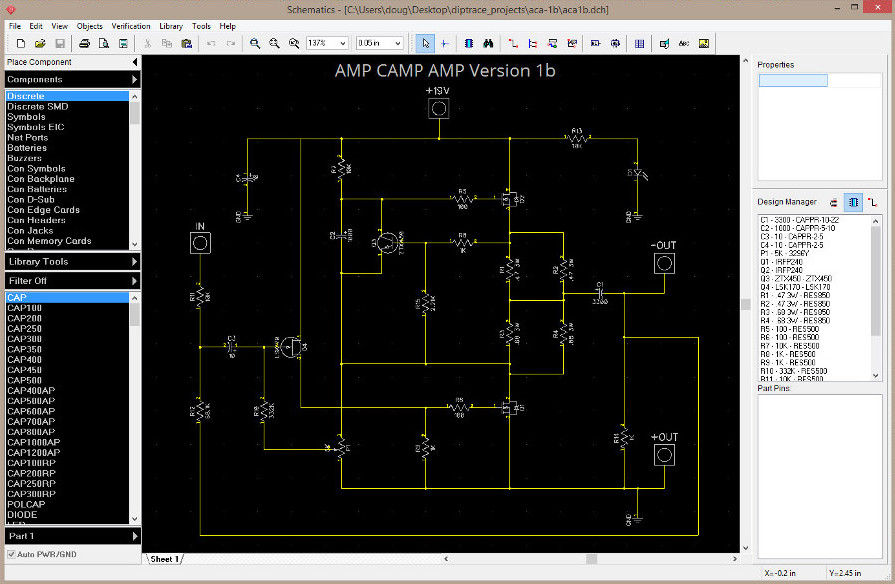
When I learned in late 2014 that Novarm had released version 2.4 which incorporated a completely new library manager I decided to evaluate the software again and use it to complete a real project I was working on at the time: a new layout of the Amp Camp Amp (ACA) #1 circuit designed by Nelson Pass.
This article aims to explain my first experiences with Diptrace and my related efforts to produce a revised ACA PCB. For more information about the chassis I developed for this PCB check out my ACA Project article.
Background
When Nelson released the circuit design for the ACA he was kind enough to provide ready-made PCBs and work with the fine folks at diyaudio.com to distribute not only the PCBs but complete kits including a monoblock chassis that leveraged an external, off-the-shelf switch mode power supply (SMPS) to provide the required 19V and 2 amps (one supply per channel).
Less than ideal for audio applications, the SMPS was clearly chosen for reasons of cost and safety, as the target for this amplifier is first-time builders. Several advanced users who decided to build the amp for fun reported improvements in sound quality and "depth", particularly at low frequencies, when the SMPS was replaced with a sufficiently capable linear supply.
Each channel of the diyaudio-produced chassis incorporated a 80x200mm heatsink which proved adequate for the design and the required 20W per channel dissipation (note: this is a 6W Class A amp and thus inefficient: dissipation is roughly 3X the rated power output), though some users reported that the heatsinks could get pretty toasty, particularly if operated in higher ambient temperatures.
 The original ACA PCB would not fit on the 2U heatsink without modifications. I did not want to move the board up since that would have covered the screw used to secure the heatsink bracket. |
 Courtesy of a diyaudio member, this closeup shows the R15 mod as applied to the original ACA PCB. Mods of this type are difficult even for those with some soldering experience. I decided to avoid it altogether. |
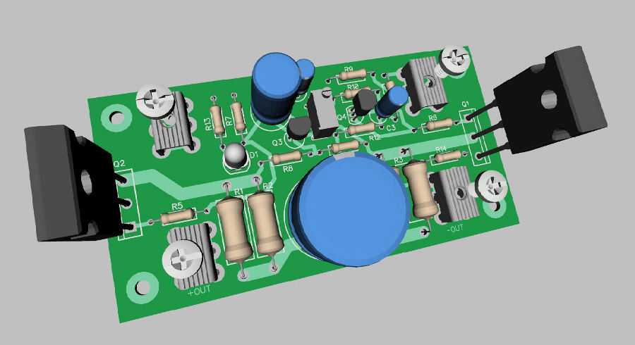
 I'm spoiling the surprise here but this is what I aimed to achieve with my PCB -- board and FETs nicely spaced on the heatsink and all mounting screws easily accessible, including those of the heatsink. |
In order to address both the power supply and dissipation issues I decided to import a 2U 300mm deep chassis from HiFi2000, known on the web as modushop.biz. This larger (but still slender) chassis provided a slightly larger heatsink (80x300mm) and significantly more internal volume as required to incorporate the dual mono linear supplies with 15V 200VA torroidal transformers, 60000uF CRC filters and soft-start board I planned to integrate.
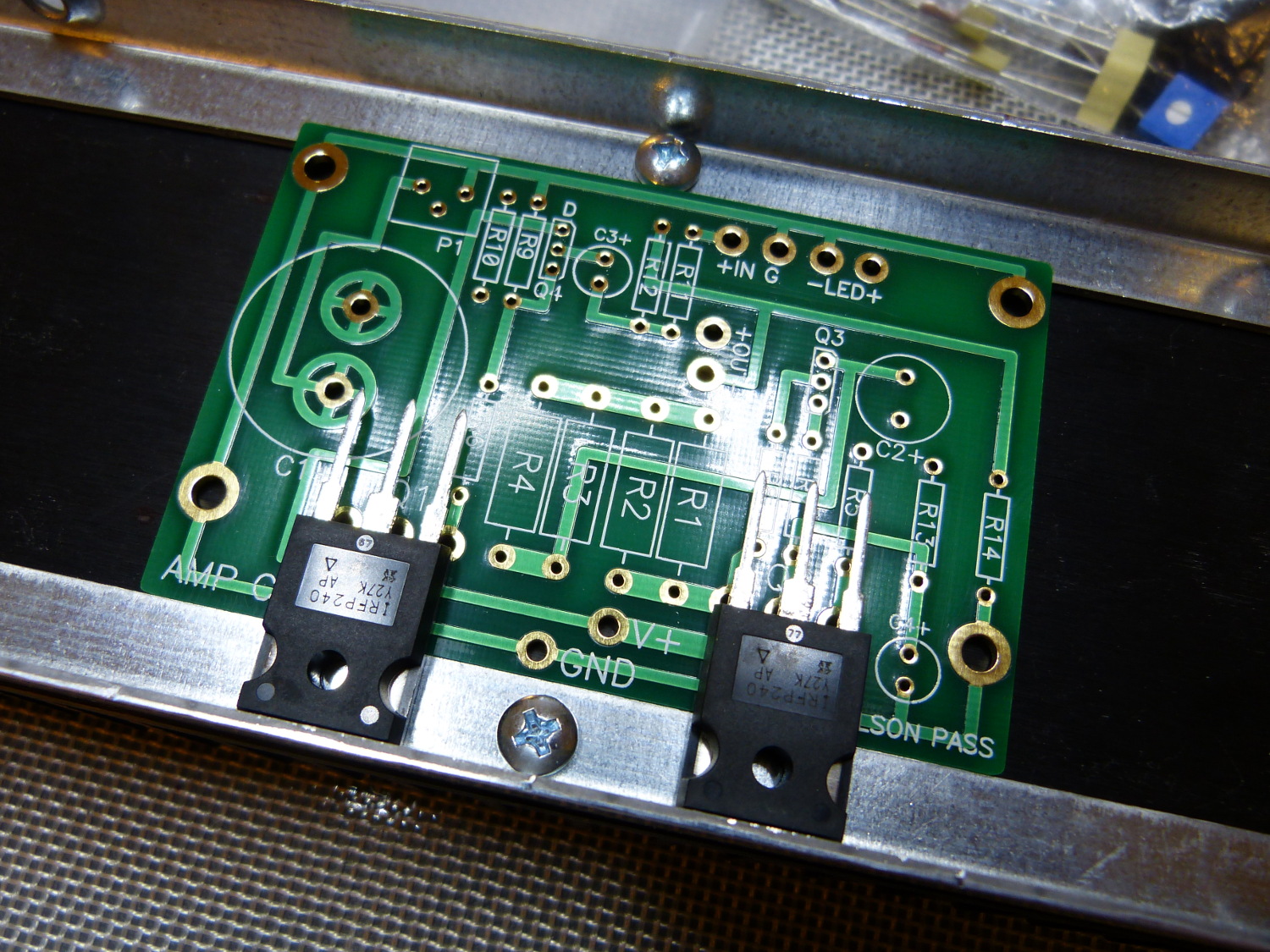
As more users began to build the ACA several noted it did not meet the original power specifications. Nelson eventually came out with a fix that involves adding a new resistor whose reference designator is R15. This version of the circuit is referred to as Version 1b.
At the time I started this project I fully expected to use the original Version 1 PCBs and apply the R15 fix but I realized I'd need to come up with a different solution for a couple reasons:
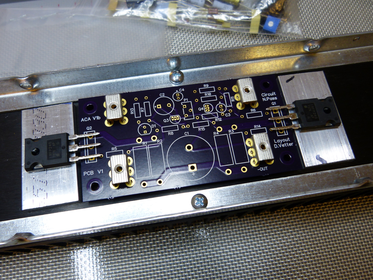
- When I attempted to orient the PCBs on the heatsink of the new chassis it quickly became apparent that the mounting rails that bind the heatsinks to the top and bottom covers would conflict with the FETs hanging off the bottom of the PCB. I could have hacked a section out of the rails to make it work but then I'd still be left with the FETS being perilously close to the edge of the heatsinks. While that's the way it's done in the diyaudio chassis primarily due to space and cost constraints, it's sub-optimal; heatsink simulation shows that for passively cooled applications it's best to position devices spread out on a centerline positioned just below the midline of the heatsink to ensure optimal dissipation. I decided to address this by relocating the FETs to the sides of the boards.
- The PCB mounting holes were constructed as vias (plated through holes) and made part of the signal ground. That's perfectly fine if you're building monoblocks (i.e. one PCB per chassis), but practically guaranteed to produce ground loops and the associated noise (hum/hiss) if two PCBs are deployed in the same chassis. I thus knew my layout would have to isolate the mounting holes / vias from the circuit ground.
While I was at it, I also figured I'd address a few other shortcomings:
- The R15 fix. It seemed wise to formally integrate the fix so that no delicate soldering technique would be required. It would also make future tweaking of the resistor value easier. Otherwise I'd have to apply the original fix which involved soldering the resistor lead directly to the lead of a TO-92 package transistor, placing it at increased risk of heat damage.
- Several people reported that the single-turn potentiometer used to set the bias voltage was incredibly sensitive and made trimming the bias difficult. I figured that I'd integrate a multi-turn pot to solve this issue. All of Nelson's other designs usually incorporate multi-turn pots so I'm not sure why he chose this part exactly but my guess is cost...plain and simple.
- While many on diyaudio espouse the benefits of single-point grounding on audio PCBs and I can relate to their arguments, as an amateur radio operator I tend look at everything as an RF project and every trace on a PCB as a potential antenna. I'm therefore partial to many of the techniques used in the design of RF equipment to eliminate radiation or susceptibility to external radiation sources. One such technique is the use of a groundplane in order to reduce ground impedance. Ground planes can also serve a secondary role as a shield but in this case I was under no illusion that would be of any value here, particularly because that function suffers considerably the second you start poking holes in the plane as required in a through-hole design. Still, my goal was to lay out as solid a plane as possible and see what happens. After all, experimentation is part of the fun.
Schematic Capture
I found Diptrace's schematic capture program to be fully functional and easy to use. The basic drawing tools worked intuitively and I never had to ask why or how something worked...it just did, and that's the sign of good application design.
The new library manager was instantly recognizable and it allowed me to quickly select components from either the standard libraries or my privately developed libraries that Diptrace calls "User" libraries. It also allowed me to easily copy patterns or components from the standard libraries into my own libraries so I could save time, for example, by reusing a standard package footprint (TO92, TO220, etc.) but incorporate my own schematic symbol and 3D model into the part. All in all this is a huge win for Diptrace and the primary reason I decided to buy a license for the tool.
Building Components
If a required component is not one of the 90K or so available in the standard libraries a custom component must be produced. I wound up building a few components and found the experience to be mostly trouble-free but not without a few challenges.
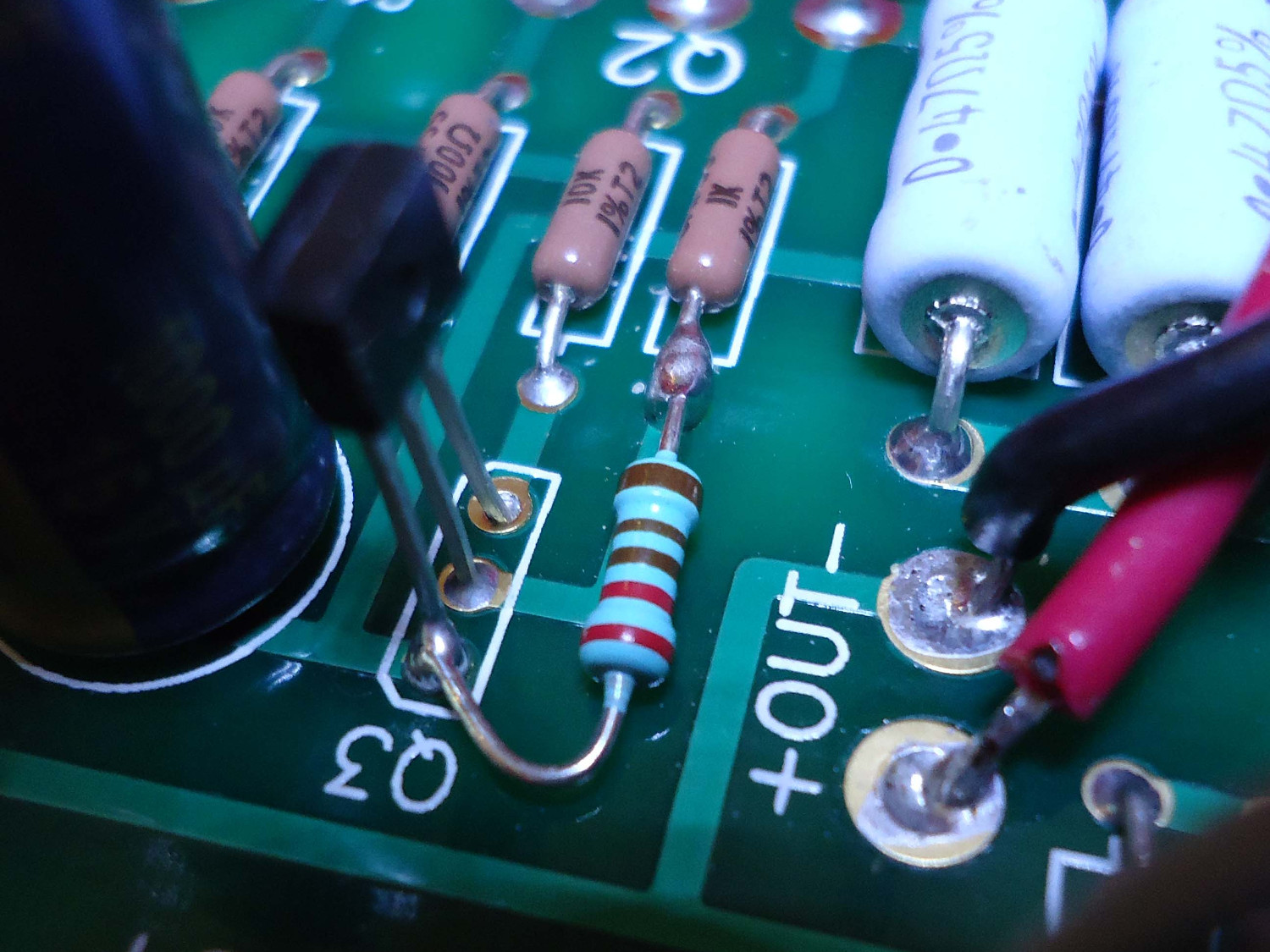
The original ACA PCB assumed the user would solder wires directly to the board but I've found that it's not particularly easy to solder heavy gauge wires that act as an effective heatsink so I decided to use a Keystone screw terminal.
I first learned about the Keystone terminals when building the diyaudio soft start board and instantly saw the benefit of these over wires or even traditional TE Faston blades. Faston blades are popular because they're inexpensive and simple but their function depends on a friction fit with their mating components. Unfortunately I have found on other projects that mating and unmating these connections places undue stress on the PCB, particularly if the blades are placed too far away from the board's structural supports (standoffs). This stress can induce fractures in the PCB substrate, lift surface mount devices off the board and, more dangerously, short through hole component leads to the chassis. Removing a mating ring terminal from the Keystone connector, on the other hand, requires only a screwdriver and places no stress on the board.
The Keystone terminal was not among the standard libraries so I had to build a custom component for it. In most cases building custom components is a straightforward process but the Keystone connector proved to be a bit more challenging. A device typically has a number of pins or leads coming out of it, each of which serve a particular function, so the goal is to create a pattern in the Pattern editor with an equivalent number of pads (for a surface mount part) or vias (for a through-hole part). Then, in the Component editor the same number of pins is created, each of which is assigned to a specific pad or via in the pattern. The problem with the Keystone part is that while it required 6 vias, all of those vias had to be assigned to the same component pin (its only pin, in fact). It wasn't initially obvious to me how to do this but some research revealed the solution: in the Component editor's pin-mapping dialog draw a rat line from the pin to the first via, and then additional rat lines from that via to an adjacent via, from that via to the next via, and so on until all vias are assigned.
I initially thought I could reuse this newly-created component for multiple signals ("IN", "+19V", "+OUT", and "-OUT") and merely change its name as required. I did in fact attempt this and managed to integrate four instances of these components in the schematic only to discover, once I'd transitioned into the PCB editor, that the resulting rats nest contained connections between these obviously conflicting signals. This was the result of the schematic program assigning all four of these connectors to the same net. That forced me to create individual components, each with appropriate names. After I replaced the old components in the schematic with the specialized versions and refreshed the design from the schematic in the PCB editor the bogus rat lines disappeared. I'm still not sure why this didn't work as expected but I got the job done anyway and there's something to be said for specializing every component -- it typically makes creating the BOM a bit easier.
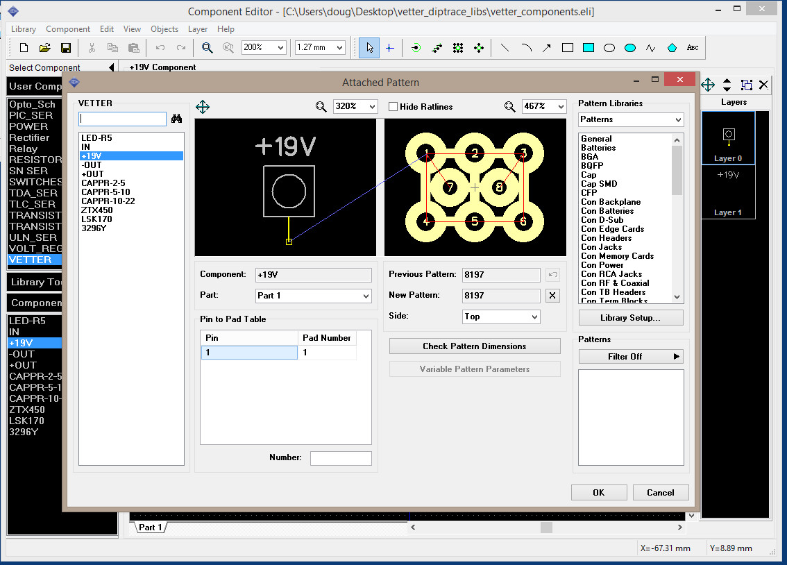 This is how I managed to map one component pin to multiple vias in the Diptrace pattern editor. The extra two vias allow substitution with TE Connectivity Faston blades. |
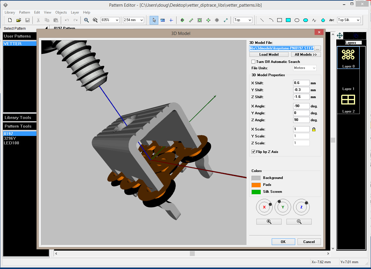 One of the best features of Diptrace is its support for importing 3D models in STEP format. I got this 3D model directly from Keystone's website and tweaked the offset values to position it relative to the pads. |
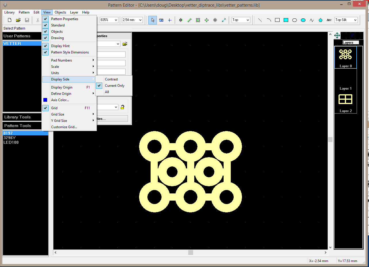 I had difficulty selecting the proper traces in my multi-layer component and changing the Display Side menu setting from Contrast to Current Only served as a fix. |
The last issue I encountered was specific to the pattern editor. It supports the concept of drawing layers so it's possibile to manipulate traces drawn simply by selecting (or merging) layers, much as you would in a common image manipulation program such as Photoshop or GIMP. The problem is that's where the similarity ends. I kept trying to select one particular trace on the currently-selected layer and that wound up selecting a trace directly below it on the Bottom layer instead. Borrowing on my experience with the aforementioned image programs I tried looking for a "hide layer" feature but never found it. Diptrace support suggested that the solution was to click once to select the top trace and twice to select the bottom trace but that didn't work to me.
I'll spare you a rant about how this is completely nonintuitive and merely offer that I ultimately solved the problem by selecting View→Display Side→Current Only. This effectively hid all layers other than the currently selected layer and allowed me to select the traces I needed. The downside? Hidden layers appear blank in the layers pane and I accidentally assumed at one point that the blank layer was the result of a previous layer merge and was no longer needed so I deleted it. I soon realized the problem and was forced to reselect that layer and recreate all the traces. Doh! My advice to the developers: gray out the content on hidden layers -- don't make the content appear blank!
The most annoying aspect of building patterns and components in Diptrace is the need to constantly switch back and forth between the Component and Pattern editor programs. While I can appreciate the reasons why the developers might prefer to keep these applications separate (simpler UI, easier to test prior to release, etc.) they're so closely functionally related that in my opinion they should be combined. I hope Novarm integrates these applications in a future release.
Forward and Back Annotation
For those unfamiliar with the terms:
Forward annotation is the process of sending schematic changes to a corresponding PCB layout program.
Back Annotation is the process of sending changes made to the circuit in the PCB layout program back to the schematic.
For this project I did not use or test Back Annotation, though Diptrace apparently supports it. I did, however, make many changes to the schematic and later send those updates to the PCB editor with ease. There are a few ways to go about this, but the procedure I used most frequently was:
- Open the schematic editor and the associated schematic (.sch) file
- Make the required changes to the schematic (add/remove/change a component type for example)
- Save the updated schematic, either by overwriting the existing file or (perhaps more wisely) adding a version to the filename
- Open the PCB editor and then the associated layout (.dip) file
- Select the menu option: File→Renew Design from Schematic→Related Schematic
If I had locked any components the application would ask if I wanted to update the locked components. Each time I selected "Yes" with no il effects...probably because I didn't make any changes to the locked components. I'm not sure what the result would be otherwise.
DRC
One of the features expected in all professional-level PCB layout tools is Design Rule Checking or DRC. Diptrace added this feature relatively recently and while it did come in handy when I was preparing the board for manufacturing I did notice a few issues.
 First, the DRC results window is
not resizeable and its contents are not selectable, hence they
cannot be copied to the clipboard for transmittal elsewhere. In
fact when trying to get help on a related issue I had to resort
to posting screenshots of the tiny window rather than simply a
textual list of the errors. I don't understand why any developer
would fix the size of a window containing variable length data.
This needs to change ASAP.
First, the DRC results window is
not resizeable and its contents are not selectable, hence they
cannot be copied to the clipboard for transmittal elsewhere. In
fact when trying to get help on a related issue I had to resort
to posting screenshots of the tiny window rather than simply a
textual list of the errors. I don't understand why any developer
would fix the size of a window containing variable length data.
This needs to change ASAP.
Second, while it's possible to double-click on an error in the results window to force the main view to zoom in on the error (what Diptrace refers to as "localizing" the error) the reverse is not true. Meaning, if there are numerous DRC errors in a particular area, depicted on the main window as a bunch of red circles, it's not possible to rollover, click or otherwise select a specific circle to obtain the error associated with that circle. I realize this might seem of little consequence but sometimes it's easier to tackle 100 errors by fixing the stuff you know how to fix first, rather than walking down a seemingly unending list (that of course can't be exposed without scrolling due to the fixed window size)
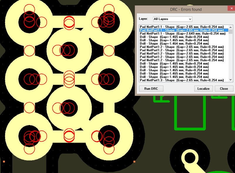
As the PCB went to manufacturing I was still unable to resolve the many DRC errors that resulted from the construction of my custom Keystone component pattern. DRC displayed probably 20 errors per pattern (80 total since I used four of those components in the design), most of which specified negative clearance values (for example "Pad NetPort1:1 - Shape (Gap=-2.65mm; Rule=0.254mm"). This error made no sense to me so I posted a question in the Diptrace Forum but at this writing had not heard back from the developers. I saw no obvious problems with the design so I ignored the errors and sent out the board anyway.
Despite these issues the DRC feature came in handy at least once. I accidentally positioned some silkscreen such that it partially covered a pad. Had this gone to manufacturing (and not been flagged by the manufacturer's own design validation process) it might have made soldering a bit more difficult. What else can I say -- DRC rules (no pun), but Diptrace's implementation could use a few tweaks.
Update: Novarm eventually responded to the forum question -- five weeks later, mind you. They said to avoid these errors I should draw only vias in the pattern editor and draw traces or a pour connecting them in the PCB editor. This is less than ideal since it means having to do this for every instance of the part in the design. I therefore consider this a workaround rather than a proper fix.
Soldermask
It's worth mentioning that, unlike more sophisticated (and expen$ive) applications like Altium, Diptrace 2.4 does not depict soldermask in the PCB editor or in the 3D view so it's harder to see at a glance whether the finished board will have soldermask in all the right places.
For example, the pattern for the Keystone connector contained both vias and traces and while I knew I wanted soldermask to be applied over the traces I initially did not understand how to ensure this would happen. I'll cut to the chase and tell you how this works:
- The soldermask layer tells the manufacturer where NOT to apply soldermask. Therefore, if there is some shape depicted on the soldermask layer, soldermask will NOT be applied there and soldering will be possible in that location assuming, of course, copper is exposed in the same area.
- Diptrace by default includes vias and pads on the soldermask layer. It does not include traces, which explains why all the traces on the board, including the traces in the pattern are covered with soldermask by default. This setting is configurable via the Gerber export dialog.
- If the goal is to eliminate soldermask over a particular area a line or polygon must be drawn on the appropriate soldermask layer. What's appropriate? If this area is specific to the part (meaning it should be repeated for each use of the part on the board) then the drawing should occur on the top or bottom soldermask layer of the pattern in the Pattern editor. If the goal is to eliminate soldermask in one or more areas on the PCB (meaning independent of the parts) then the line or polygon must be drawn on the top or bottom soldermask layer in the PCB editor.
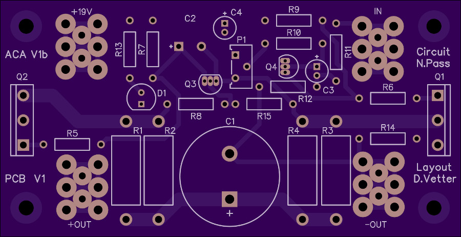
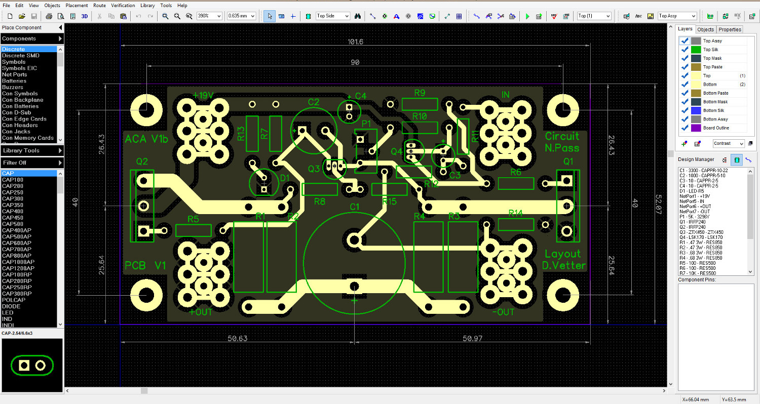 The top layer of the ACA PCB showing the board outline (purple rectangle) and related dimensions. The mounting holes are slightly wider than the original PCB to accommodate the Keystone connectors. |
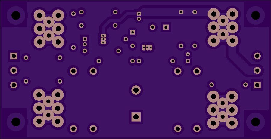
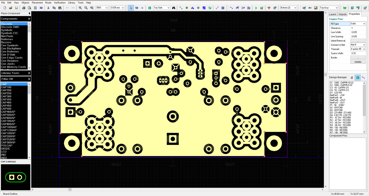 I took a chance and integrated a copper pour on the bottom layer to serve as a ground plane. Notice the Keystone connector on the bottom left is tied to the pour through 90 degree 4 spoke thermals to make it easier to solder. |
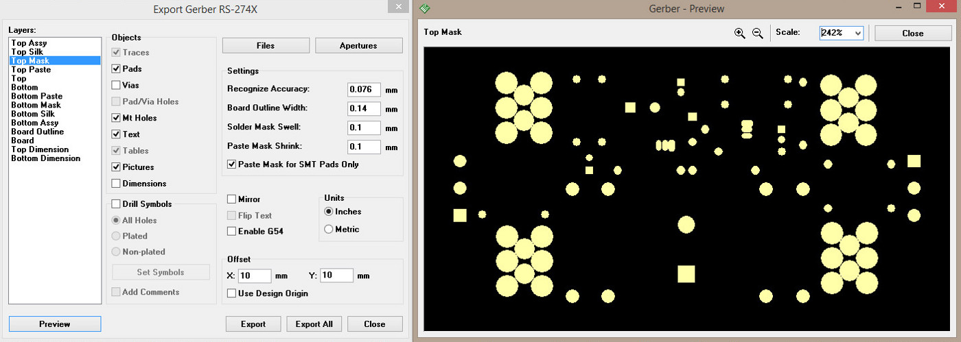 Diptrace's built-in Gerber export capability and preview mode is shown here. In the right side window I'm previewing the Top layer soldermask. Note how the traces on the Keystone pads are not exposed. That means they'll be covered with soldermask. |
I learned most of this while reading a forum post related to the creation of thermal pads for a surface mount device. In this case the user drew a polygon with the required dimensions on the top soldermask layer in the Pattern editor and found this to work as advertised -- the thermal pad was left bare so it would bond to the underside of the device during the the reflow process.
Incidentally, the mounting holes for this board were created as static vias rather than standard mounting holes because vias help provide additional support to the fiberglass substrate. However, Diptrace by default kept soldermask over them because they were not connected to any net. That setting can be tweaked when generating the gerbers.
Generating Gerbers
Selecting File→Export→Gerber... provides a means to view each layer of the design and save each layer to individual files that are required for manufacturing.
After working on a board for a few days or weeks in a nicely rendered CAD environment it's easy to become complacent and believe the Gerbers will result in a board identical to that depicted in the editor. However, as I already indicated, Diptrace does not render soldermask in the PCB editor or 3D view properly so it's essential to examine each layer of the design using the Preview feature on the Gerber export dialog to ensure the board will be manufactured properly. It wasn't until I did this, incidentally, that I understood exactly how Diptrace generates the soldermask layer.
The ACA board was a simple two layer design (copper on top and bottom, no internal layers) so I specified the generation of the following layers:
- Board outline (including dimensions)
- Top silk (silkscreen)
- Top mask (soldermask)
- Top Layer (signal)
- Bottom Layer (signal)
- Bottom mask (soldermask)
- Drill File (defines the size and locations of holes to be drilled)
I had no components on the bottom of the board, hence no reference designators or other writing on the bottom of the board for that matter, so I did not need to include a bottom silk layer.
I then wrapped these files in a zip file and uploaded them to my manufacturer.
Selecting a Manufacturer
I considered sending the design to Advanced Circuits, a company I have some experience with at work called TTM and a few others but I wound up sending the design to OshPark for several reasons:
- No panelizing required (meaning: fewer coasters if this turned out to be a dud)
- Reasonable minimum order (Qty 3, additional boards available in multiples of three)
- ENIG finish. Harder to solder than immersion silver but less susceptible to tarnishing
- Purple soldermask: Not my cup of tea but not the same old boring green stuff either
- Cool website that renders the board design so it can be reviewed before ordering
- Boards separated (no need to come up with a V score or breakaway tab strategy)
- Made in the US (not just a US front company that sends everything direct from China)
- Cost: $45
There were a couple downsides to Oshpark however:
- Lead Time: (10-12 days). This is due to their need to fill out a panel with other projects before it is sent to manufacturing.
- No 2oz Copper option: High current applications like audio amplifiers benefit from heavier copper traces but I wound up accomodating this by recalculating the trace widths for the high current sections and ensuring they would be sufficiently wide.
Both of these issues were more than offset by the positives and so I had no reservations at the time I placed my order. For what it's worth, the panel to which my PCBs were assigned was sent to manufacturing three days after I placed the order and the finished boards shipped to me from Oregon eight days later, so their estimate was accurate.
OshPark rendering of ACA V1b V1 PCB Top Layer
OshPark rendering of ACA V1b V1 PCB Bottom Layer
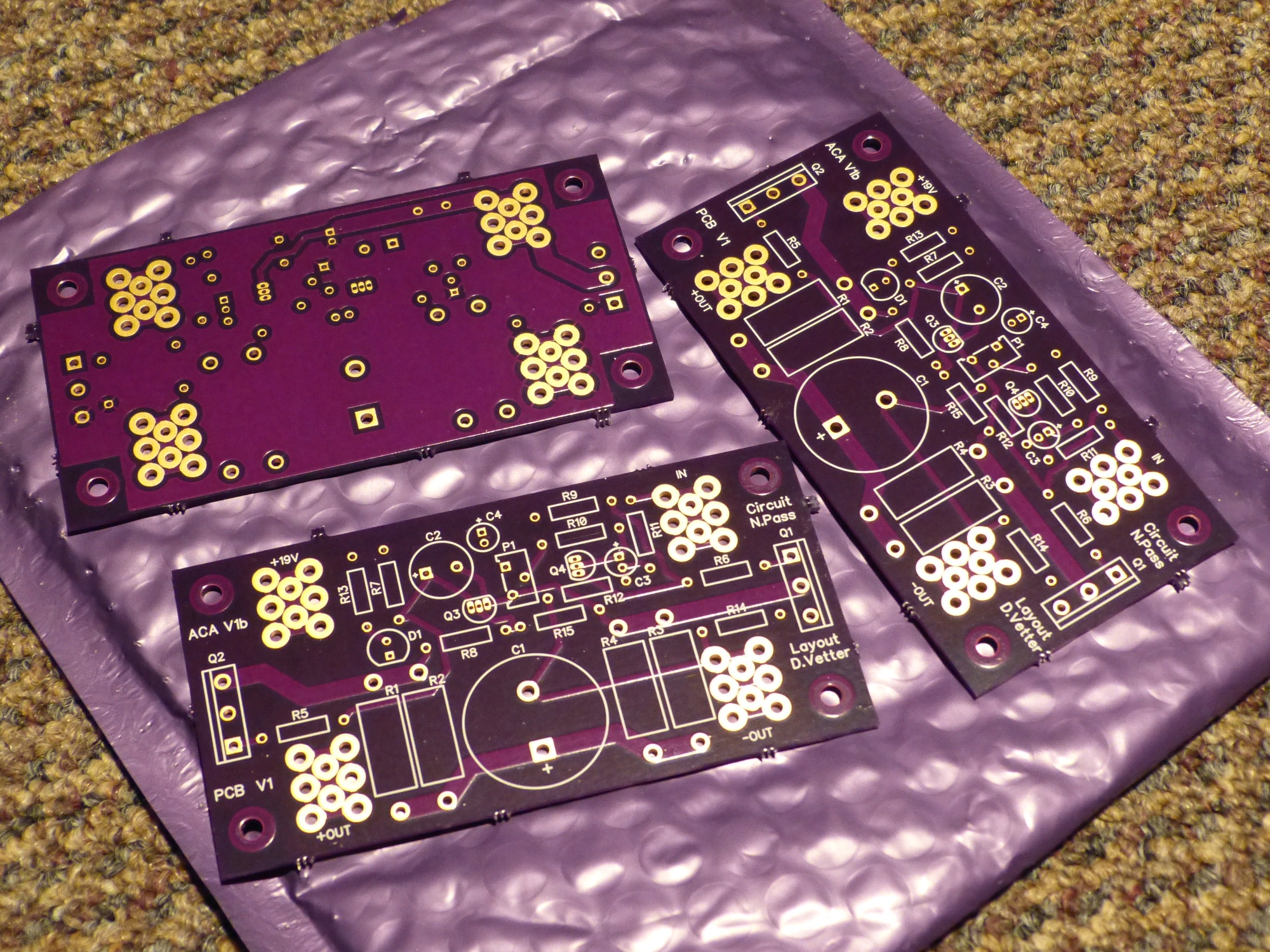
Three boards delivered from OshPark in roughly two weeks (in
purple bubble wrap too!)
Critical Feature Lacking in Diptrace: High Speed Support
I bought Diptrace primarily to gain experience in the manufacturing of analog and relatively low speed digital designs, and in that sense it's delivered and I'm glad I spent the money on a Standard license (4 signal layers, 1000 pins).
The problem is almost every digital design I have planned from this point on will require USB, Ethernet, or other high speed transports. These function using differential pairs that require PCB traces that conform to several requirements including matched length, width, impedance and clearance to other traces. As I see it, the single biggest failing of Diptrace 2.4 is its complete lack of support for differential pair routing and high speed layout in general. To remain relevant in the modern age it must include these features.
The upside is that Novarm posted in their forums in the latter half of 2014 that they had recognized customer demand for these features, to the point that they shelved some work they had previously scheduled to get started on high speed support. They promised basic high speed features in the next release "by the end of the year", but as the old joke goes "what year?" 2014 left us without so much of a whisper from Novarm. Let's hope they deliver before the end of 2015.
Conclusion
Diptrace is probably the best Schematic Capture and PCB Layout program available for the money. Its continually developed and its developers have a history of listening to their customers. They also have the most customer-friendly licensing policy in the industry. The big players (I'm looking at you, Altium) could take a few lessons from Novarm. Put simply:
- The software is licensed by the number of pins and signal layers rather than the physical board size. Ground and power planes are unlimited.
- An upgrade of the license type costs only the difference in price between the two licenses. Going from Lite ($145) to Standard ($345)? You're on the hook for only $200, not that plus some stupid 50% "upgrade fee" or other horseshit the big players charge you for the privilege of giving them more of your hard-earned money.
- All minor releases within a major branch (2.3, 2.4, etc.) are free. Upgrades to the next major release (2.x→3.0) costs 50% of the original license fee, so if, for example, Diptrace provides high speed support in 3.0 I'll have to pay $172 (and change). That's fair because it rewards Novarm only if they produce features for which users are willing to upgrade.
Diptrace is not without its issues, however:
- The aforementioned lack of high speed layout capability is a serious limitation. High speed layout is no longer strictly the domain of professionals engaged in the business of manufacturing printed circuit boards. Even hobbyists need a means of laying out high speed transports.
- I found technical support a little slow to respond, and found the forum was no substitute for a properly trained support engineer. The lack of a ticket system is also frustrating, and may in part explain why support requests are answered slowly or not at all. I realize this may be a simple matter of "you get what you pay for". For the record, I'd pay a little more to get better support, particularly if the support staff were within a couple timezones of me.
- Releases occur randomly and relatively infrequently (2.3→2.4 took almost two years). There is also no effective communication about the current and future release cycles so I'm left to guess when high speed support will be available, for example.
I had planned on buying a copy of Altium to address my high speed layout needs and I may still do that but if Novarm can deliver an 80% solution soon (differential pair support and related DRC functionality with push-shove routing to follow) I may be able to save myself thousands and get my work done in Diptrace.